PCB process identification
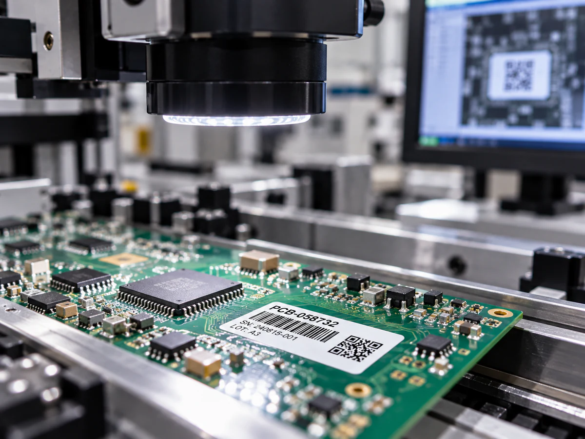
Place the identifier in an agreed keep-out area, clear of contacts, components and tooling. Record whether labeling happens before or after soldering.
01 / Industry application
PCB and electronics identification through assembly, soldering, cleaning and inspection, with process-specific constructions and compact traceability.
02 / Where labels work
Board identity needs to survive the steps between bare-board labeling and final test. Label placement, heat exposure and reading geometry must be resolved before a code format is chosen.
Place the identifier in an agreed keep-out area, clear of contacts, components and tooling. Record whether labeling happens before or after soldering.
Link a board serial to the panel, process lot and inspection record; plan how panel separation affects the identity.
Housing labels can carry model, rating and service information under a different construction specification from the board-level process label.
03 / Process and service
Map SMT reflow, wave solder, flux contact and cleaning in order. A brief peak, repeated passes and sustained service temperature represent different demands. Small label areas also constrain code density and print quality.
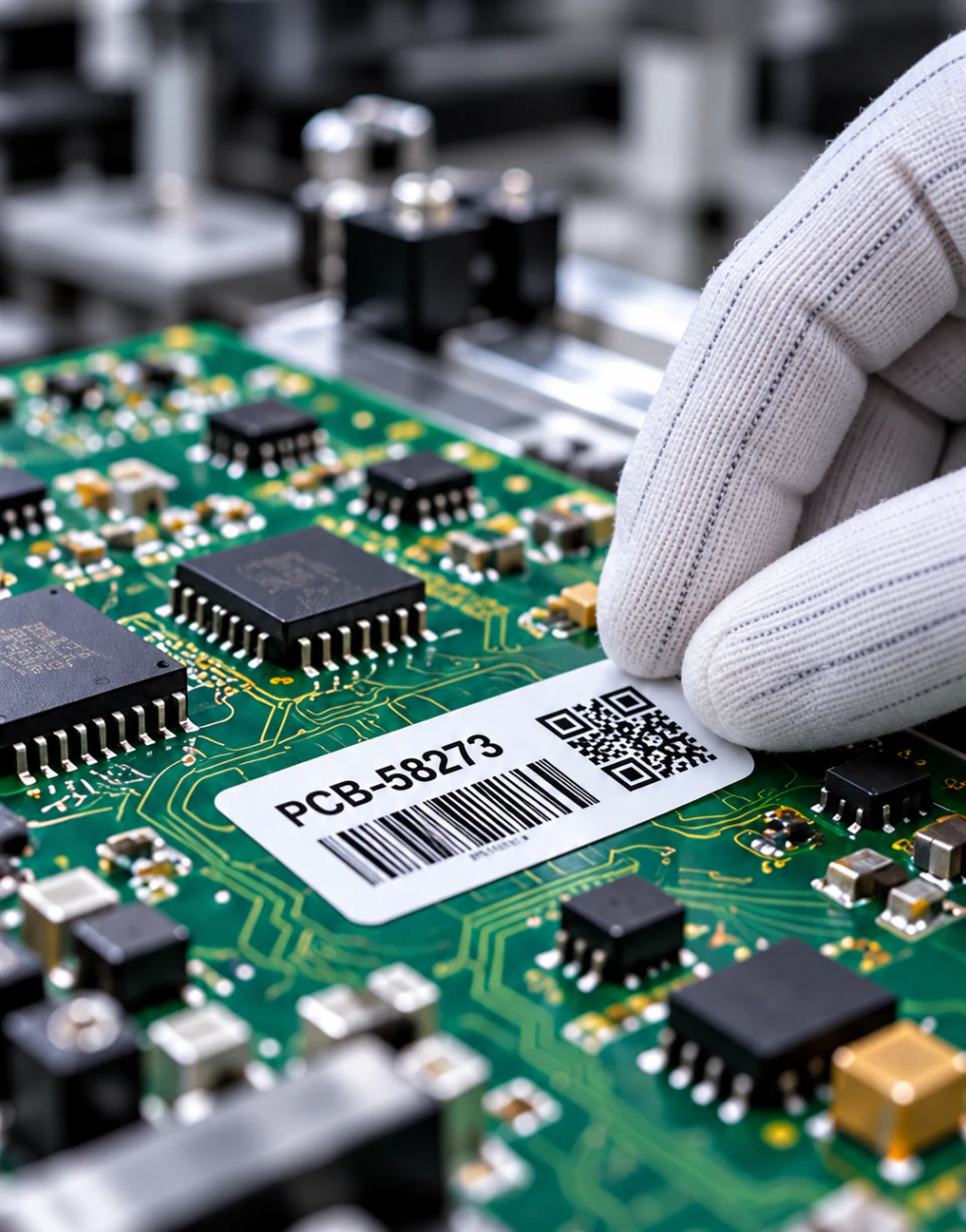
Label placement must preserve the board identification area and component clearance.
05 / Material, adhesive and identification
Board and assembly serials support WIP, inspection and final-test traceability. Agree data uniqueness, human-readable fallback, print resolution and scanner geometry before locking the artwork.
RoHS, REACH and halogen-free documentation may be project requirements. ESD-sensitive assemblies require a separately established construction and handling specification; PI alone does not establish ESD performance.
Run labeled samples through the actual profile, including repeated passes and cleaning. Read codes before and after processing using production equipment and inspect adhesive movement, lifting and print change.
06 / Start a conversation
Share what you already know. We can work through the remaining details together.